With the progress of leading edge semiconductor micronized technology, the chips further integration, acceleration, and less power consumption progressing every year, and it will become a huge driving force in pushing for electronic equipments miniaturization and increasing sophistication and high performance.
However, on the other hand, this has given a huge effect on the assembly method, printed circuit and printed wiring board for effective and stable chip circuit connections; the printed wiring board is evolving rapidly in recent years.
Additionally, assembly is explained as a method that enlarges input output signals of chips with superfine circuits to an actual usable size without failing its functions and based on assembly, the circuit elements are connected to be made into electronic circuit modules and construct electronic equipments.
Therefore, to bring out the acceleration and further integrations of the chip properties, substrates with high wiring density will be necessary. Recently, the multi-pin, narrowing terminal pitch and micronization of the chips are accelerating every year, and for semiconductor package substrates that utilize this requires higher technology and reliability than before including additional micronization and high concentrations of wirings, and narrow width of the through hole pitch.
As a member of the semiconductor industry, our company is involved in research and development related to manufacturing technology including package substrate innovative techniques and new products to improve productions in order to respond to clients' diversified and sophisticated needs, and while polishing our expertise in thin type, high-density technology in the coming years, we are carrying out R&D activities in innovative technology and techniques research and development as our basic policy that are able to answer to clients' diversified and sophisticated needs.
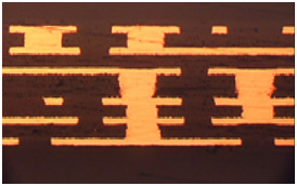
1. Fine Pattern Shaping
- Recently, a remarkable progress is seen in substrate micronization. At our company, while pursuing micronization using subtractive method (※1) which are a conventional method, we are also researching micronization techniques based on the semi-additive method (※2) that has recently established its effectiveness.
Currently we have reached the research and development level of L/S=15/15 um micronization.
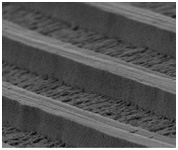
L/S=25/25um
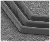
L/S=20/20um
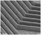
L/S=15/15um
- ※1. Subtractive Method
A method of forming a copper circuit pattern by shaping a dry film layer on a copper clad laminate created with a copper thin layer on a resin substrate, then, after printing the circuit pattern, an edging process is carried out where lined copper parts other than the circuit are removed. - ※2. Semi-additive Method
A method of forming a conductor pattern by first, thinly plating the surface of an insulation board not lined with copper foil with electroless copper plating, next, coat the resist and later thickly plating only the conductor pattern with electrolytic copper plating and carry out edging after detaching the resist after plating.
2. Ultra Fine Hole Opening Finish
- In a progressive miniaturization, thinning and compacting of electronic equipments, even for build-up layer semiconductor package substrates, the requirements for increasing circuit micro wiring and through hole pitch narrowing width are soaring.
Substrates have through hole in their core layer, and when it has a large projection area compared to the wiring width, the transmission properties deterioration is thought to be higher due to the signal line with increased conductor resistance through thinning and loaded grounding capacities. - Our company will solve the problem by establishing ultra fine hole opening technology.
- Development Target: Hole Diameter 30-50um
※Under development, using state-of-the-art laser
3. Ultra-thin Multi-layer Board
- In order to respond to the requirements of high wiring density, build-up structures are necessary for package substrates. Accompanying chip miniaturization, thinning of board thickness, and finer wiring has become a necessity in build-up structure multi-layering substrates.
- Our company is involved in ultra-thinning multi-layer boards that have solved electrical problems.
- Development Target: Total Board Thickness 180um(4 layer board)
※Using ultra-thin core material, ultra-thin PREPREG
1/2/1 B/U 4 Layer Substrate
2/2/2 B/U 6 Layer Substrate